Understanding Stop Mask Expansion
Stop mask expansion is an important PCB detail, and responsible for declaring how much “extra” area is exposed next to your solder pads.
Mask expansion helps your design cope with fabrication tolerances, ensuring that normal fabrication doesn’t cause assembly issues. A properly set mask expansion ensures that your PCB can be reliably and consistently assembled across large numbers of orders and build processes.
Recommended Mask Expansion Setting
When in doubt, we recommend following these settings:
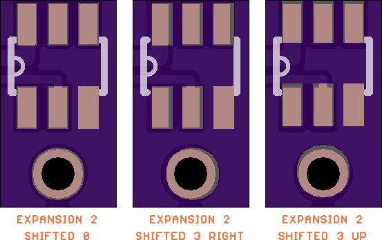
For 2 layer boards, use a mask expansion of 2mil (0.0508mm).
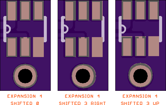
For 4 layer boards, use a mask expansion 1.5 mil (0.03810). You can also set your mask expansion to 2 mil, but if you do so we recommend adjusting the isolation of copper pours and ground planes to 6mil (0.1524) or larger.
These values correlate with a fabrication tolerance of 3 mil (0.0762mm), which covers expansion, retraction, and shift.
Examining the effects of Mask Expansion
Even if you’re not familiar with PCB terminology, this image should help explain the effect of mask expansion
As you can see, as the stop mask expansion increases it starts causing noticeable issues. However, because of other fabrication tolerances, stop mask expansion can cause problems at much smaller values than before they’re apparent on previews, like you see here.
For the purposes of demonstration, all the images here are presented with the following unless indicated:
- Mask expansion as specified in the image
- Copper clearance of 6 mil, as you would see on our 2 layer boards
- Specified units are in mil, which is equal to 0.001inch, or 0.0254mm
Problem: Irregular Pad Size/Shape
You can see this on the lower right pad. This mostly affects with ground planes and no thermals. It can also affect boards with large power traces. You can also see this on the top left, which is “longer” than the other pads.
Because these pads do not have a break in the copper around them, the soldermask is the only thing that defines the pad size. As you increase mask expansion, the pad larger or misshapen. This can result in issues when using reflow assembly, since the pad will have different solder flow and surface tension.
Problem: Exposed ground planes and traces
You can see this on all pads, notably the lower-left.
The mask expansion extends beyond the copper isolation, and exposes nearby ground planes and traces. This severely impacts ease of assembly These boards are nearly impossible to hand-solder, since it’s very likely you’ll accidentally bridge the ground plane to your pads.
When assembling with reflow, this is less of an issue, as the solder paste will typically avoid bridging. However, bridging can still happen, making large, complex boards very difficult to troubleshoot.
Calculating optimal values
In general, you can calculate the maximum mask value by this equation: (mask expansion) < (copper isolation) - (mask tolerance). The ideal mask expansion is as large as you can make it while honoring that equation.
For our 2 layer services, this means (mask expansion) < 6mil - 3mil. This is how we derived our suggested value of 2mil, giving 1 mil of extra space to ensure the copper is fully protected.
For our 4 layer service, the copper clearance is 5 mil. (mask expansion) < 5mil - 3mil. A mask expansion of 1.5mil is thus recommended over 2mil, to ensure that the edge of the ground plane is not exposed.
For 4 layer boards with very fine-pitch components, you may wish to have a larger mask expansion. In these cases, it’s recommended to adjust the copper isolation, or carefully inspect the design to avoid potential issues later on.
Mask Expansion and Tolerances
Like any physical process, every fabricated PCB will have small variations in size and shape of the soldermask. Mask Expansion, when set correctly, prevents these small variations from impacting your design.
0 mil with tolerances
For almost all boards, a mask expansion of 0 works perfectly fine. This image shows how your board is affected by these tolerances being applied. Effectively, the only issue is that you “lose” some space on the edge of your pad (up to 3mil). This won’t cause issues unless you’re both unlucky and using fine pitch parts such as TQFP, BGA, or 0201.
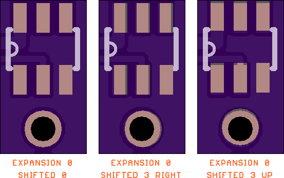
2 mil with tolerances
Our recommended value works well for almost all cases.
For fine pitch parts, mask shift allows you to lose 1 mil during shift, but this is only a problem on very specialized footprints. However, the mask shift doesn’t exposes nearby ground plane to soldering, which is the important detail.
Bad values
Calculating Bad Values
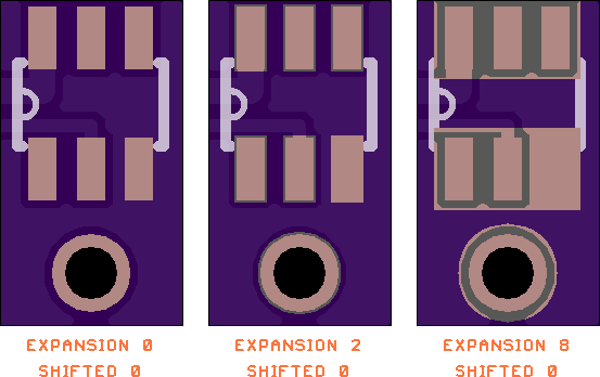
4 mil with tolerances
4 mil is where problems start happening. As you can see on the image, the previews themselves look OK, except for the large pad.
However, on a fabricated board with maximum tolerances, you’ll see that the mask starts exposing traces and ground planes. This is because at 4 mil, the combined values for mask expansion and the mask expansion tolerance exceed the copper clearance.
Because this depends on the exact tolerances of a particular PCB, issues will be uncommon and sporadic. It’s common for boards like this to be fabricated without issues a few times, only to go to production and realize a lot of boards have potential faults.
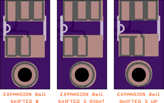
8 mil with tolerances
Since 8 mil expansion is already bad, adding tolerances doesn’t make it much worse. You can see here though, that the mask shift potentially makes it even easier to accidentally solder bridge to ground planes and traces.