Inverted Gerbers
In addition to internal file format, Gerber files also have two different ways to draw the gerber, that affect how the layer is intended to be fabricated. These are typically known as “positive” gerbers and “negative” gerbers. Most layers have a de-facto standard for fabricating that layer, the internal planes often vary based on the design tool setup and fabricator.
For our production process, we only use Positive gerber formats for all copper layers.
Converting Negative Gerbers to Positive Gerber Format
Converting between formats is often non-trivial, and it’s far more reliable to produce Positive gerbers from the design tool when placing an order.
Most major design tools produce Positive and Negative gerbers based on the Layer Type for each copper plane. If the Layer Type is set to “Signal”, then the design tool will produce Positive gerbers, which are suitable for our production. If the Layer Type is set to Power, then it will produce Negative gerbers, which will not work with our process without correction.
Correcting this is usually a simple process.
- First, the Layer Type must be changed from Power to Signal, which forces generation of Positive gerbers.
- Add a copper pour to the internal plane
- Set the copper pour to the correct net for your power signal to connect it ( such as GND)
This process has been confirmed on several design tools including Eagle, Altium, Proteus, ORCAD Allegro, EasyPC, DesignSpark, and Diptrace.
For internal planes with multiple sections, internal traces, or isolated regions, converting the layer type might be very difficult. In these cases, please email us at [email protected].
Positive Gerbers
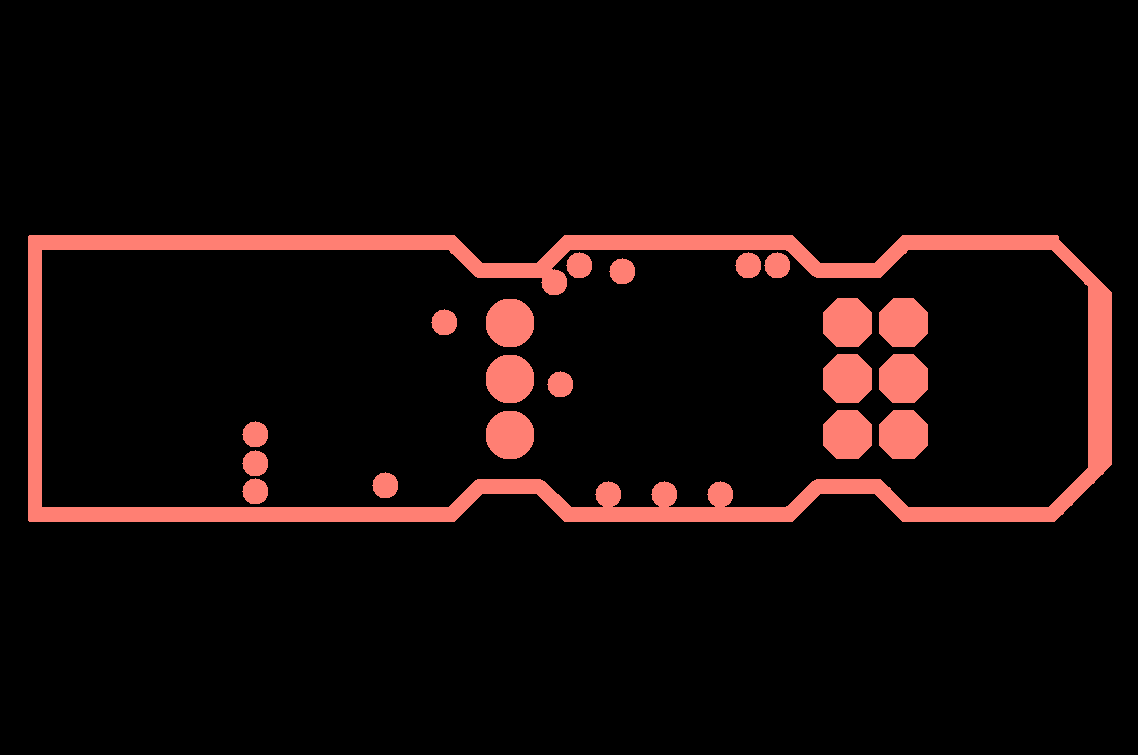
Positive gerbers indicate where the fab should leave copper on the resulting PCB. This is the format that we expect for all internal copper layers, as well as the top and bottom layers.
In a gerber viewer and on our site’s previews, you would see the ground planes and any traces indicated as a colored region, similar to the picture below. Any disconnected vias will be rendered as a isolated trace (as shown here) or as a black dot.
Negative Gerbers
Negative gerbers indicate where the fab should remove copper. If your design tool is generating Negative gerbers, please read the section above for converting to Positive gerbers.
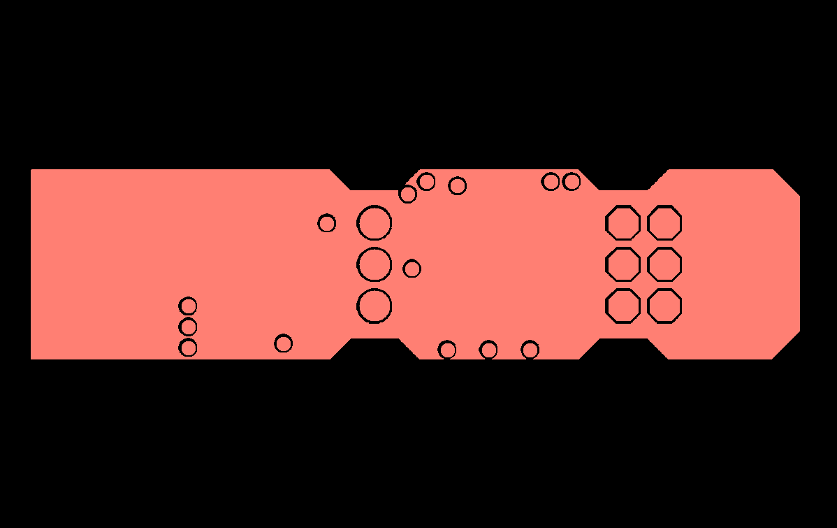
Negative internal planes typically appear similar to the picture below, with only the edge clearance and via isolation being shown. If your internal connection have thermals, you may also see an X or + mark around connected vias.
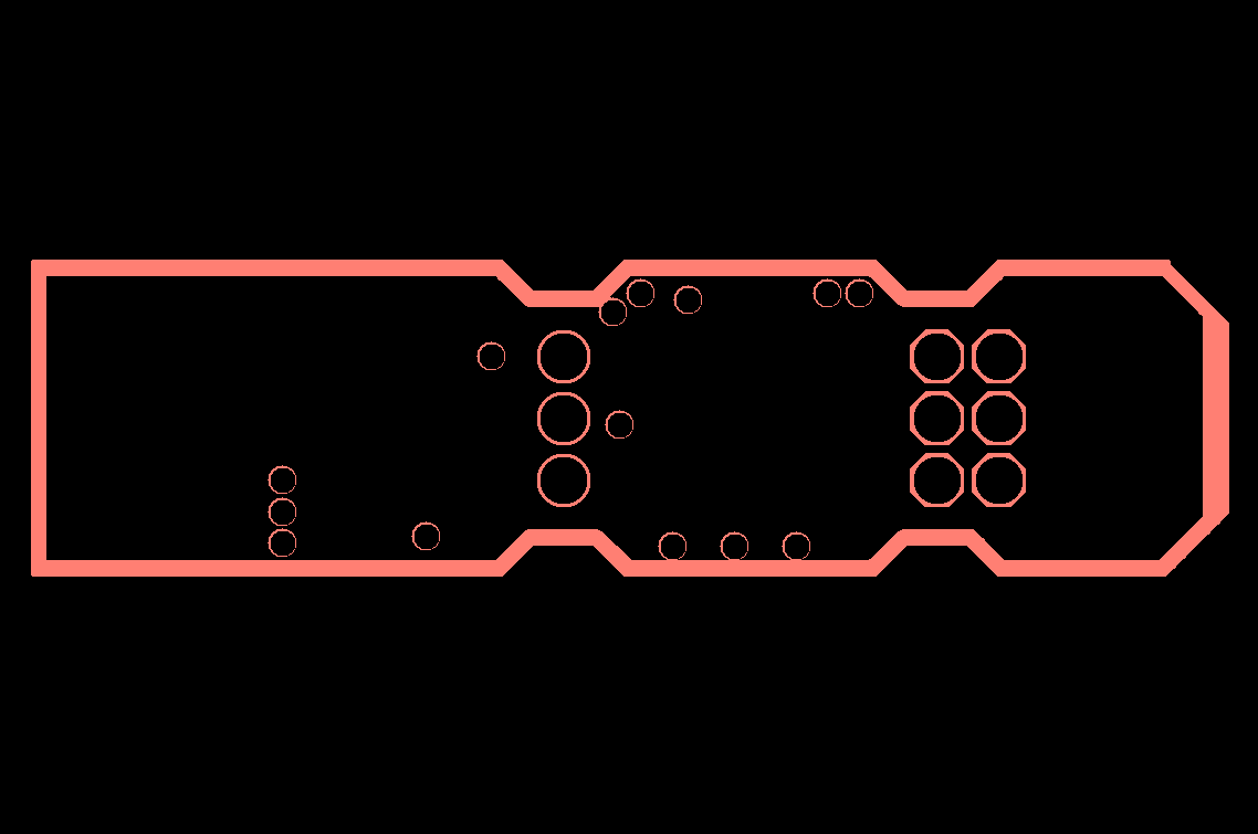
It’s also fairly common for Negative internal planes to simply not have copper around disconnected vias, which renders similarly to the picture below.