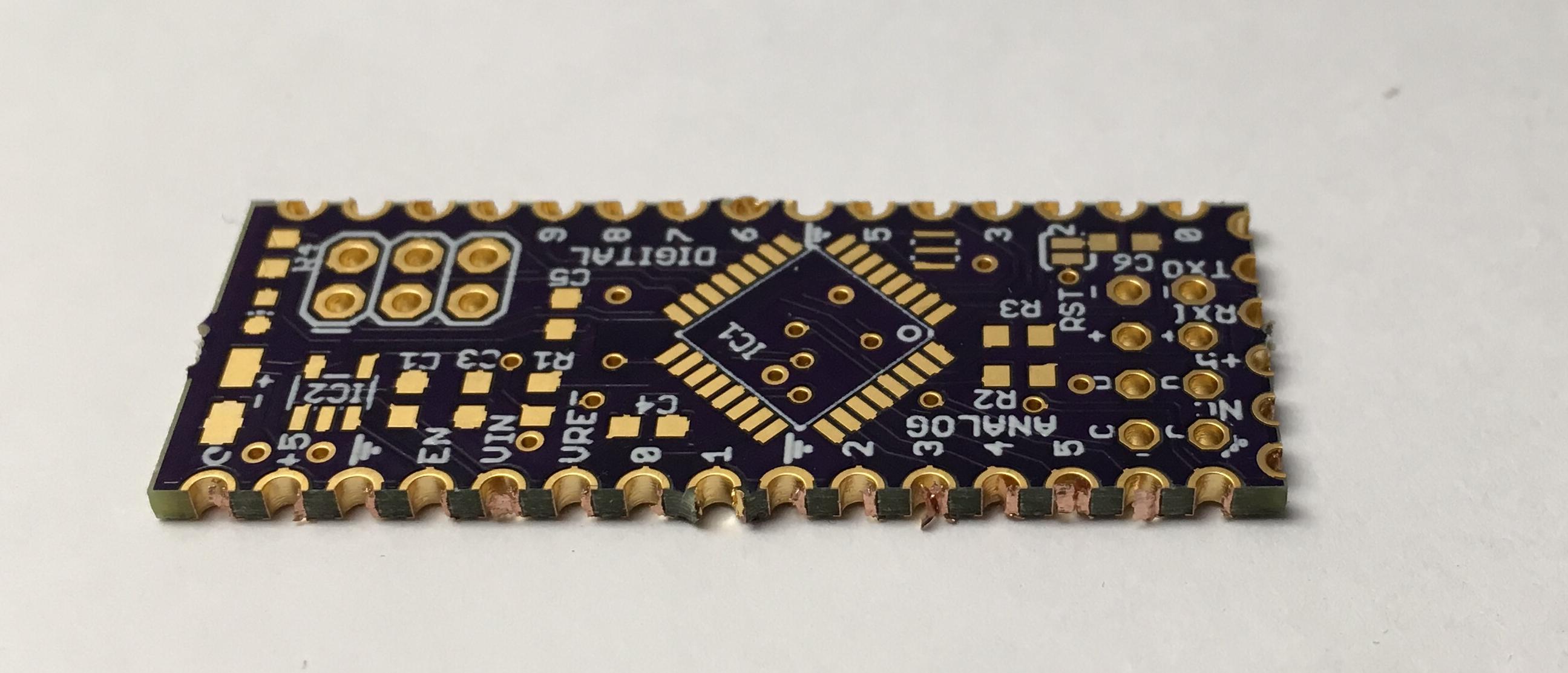
Castellated Edges
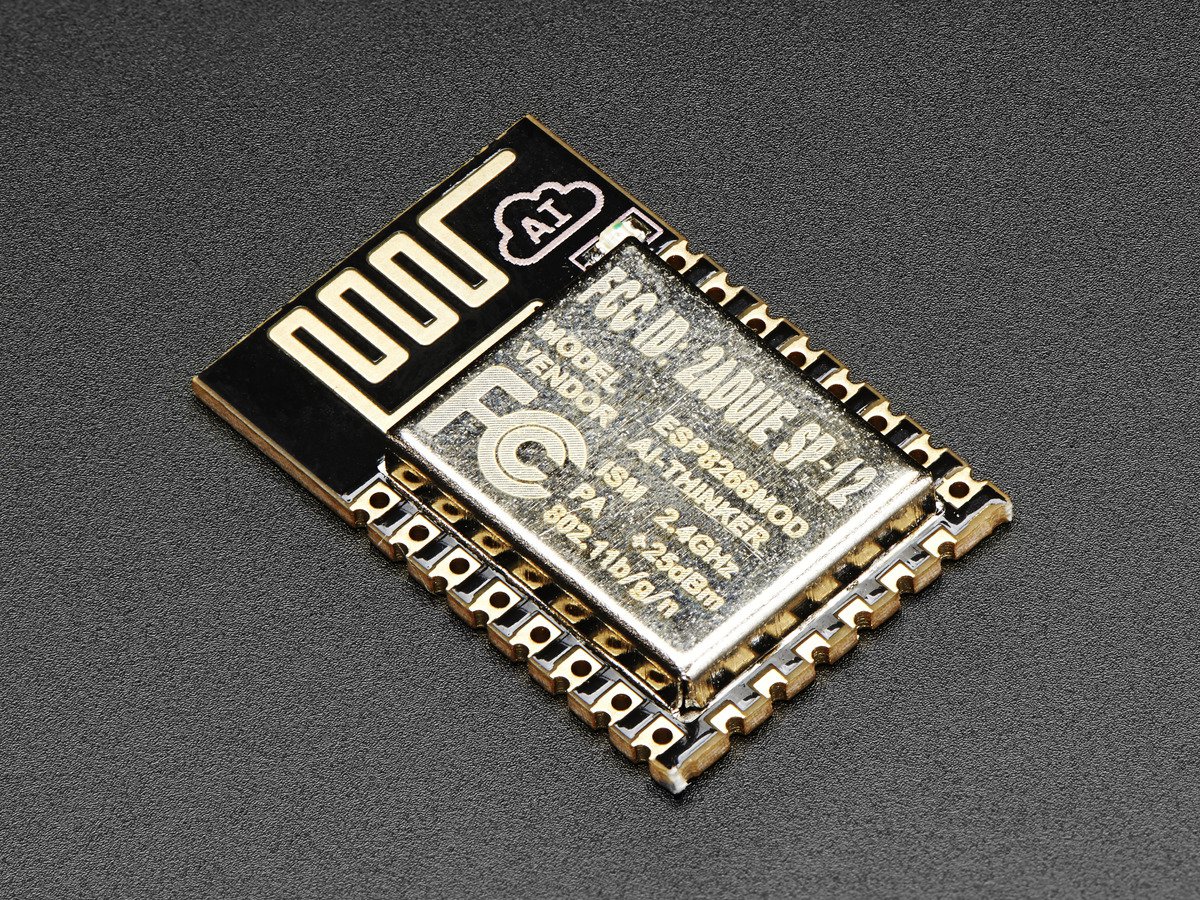
Castellations are small plated edges, typically used for making circuit boards into small pcb modules. These are often seen on wireless modules, such as the ESP8266-12E.
While we don’t offer full support for castellations, they can be fabricated if you don’t mind a few minutes of rework and verification of the PCBs.
Design Considerations
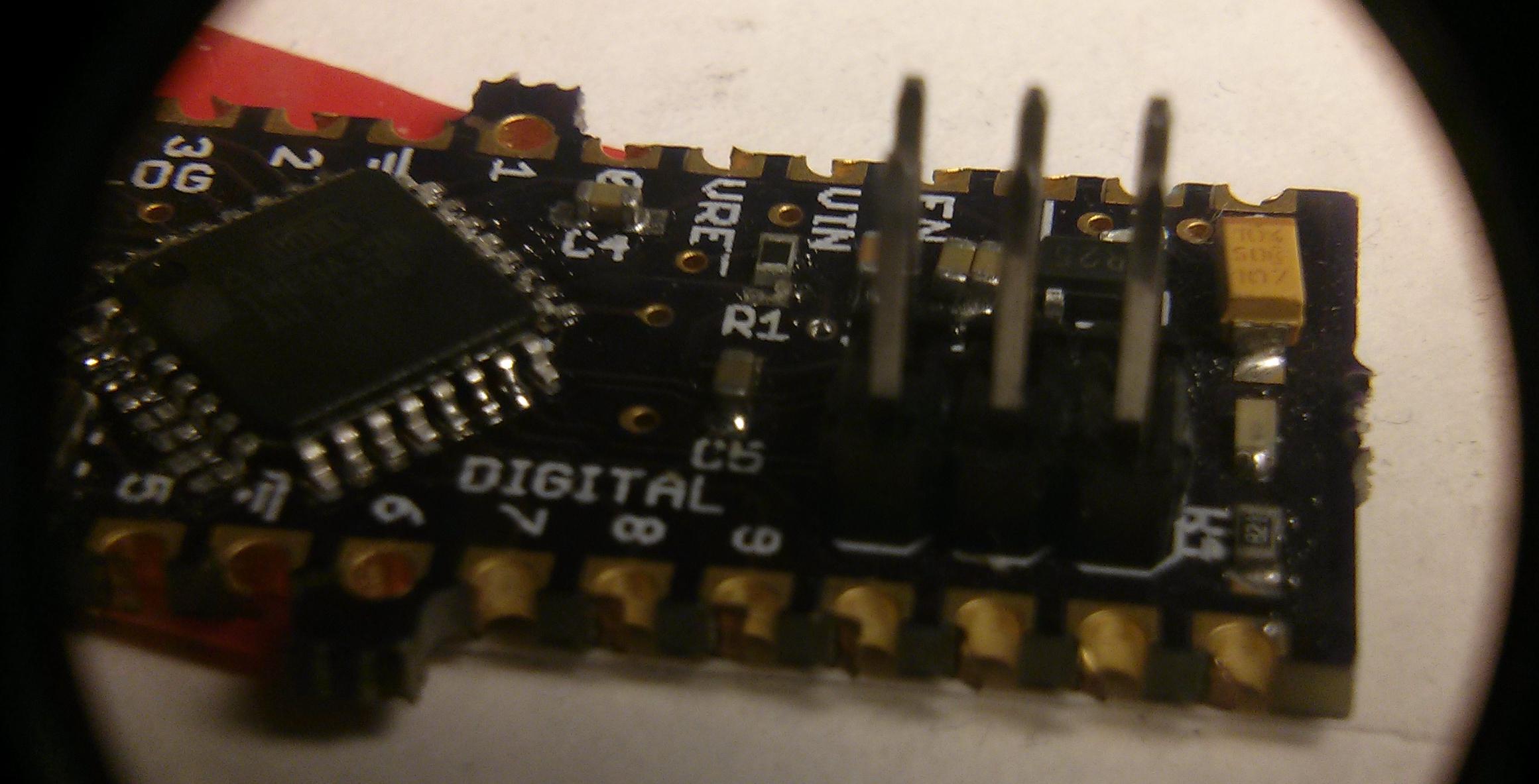
It’s helpful to include a fallback hole near the edge. The ESP8266-12E boards, are a great example here. The extra via allows easy connecting of wires for rework, and makes it easy to salvage a module if the fabricated PCB doesn’t turn out perfectly.
Indicating in the design file
Castellations are simple to call out in most design tools. Simply include a via on the PCB, so the board outline goes through it.
However, due to our panelization process, the castellated vias must be indicated with round pads for copper and stop mask. The pads must also not extend more than 40 mil from the board edge. Square pads or pads that extend far beyond the edge will be trimmed, and the via will not be plated.
It’s also helpful to use a 10 mil wide line for the board outline. With our milling tolerance of 5 mil, this provides a good visual indicator of where the physical board edge might be. The fabricated edge can be anywhere within that line. This is very helpful for fine-pitch castellations with smaller holes.
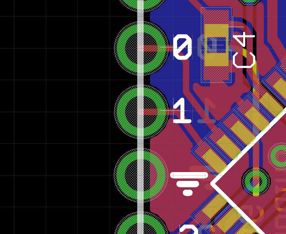
Rectangular castellations can be made by using vias with round pads as noted above, and adding overlapping rectangular SMD pads. Since these pads are inside the board outline, they will not be trimmed, and will provide additional area for soldering (see below for example).
Cleaning up the final boards
We make a best-effort to minimize support tabs on castellated edges, but it sometimes happens. In these cases, you’ll need to file the tab off of your edge.
Additionally, the via plating may not be fully removed during the milling process. In some cases it’s smashed next to the edge, where it can cause unwanted connectivity between vias. In others, it’s smashed inside the via, where it will prevent good solder flow. A fine point file or hobby knife will help remove excess plating.