Design Rule Setup
The design rules describe manufacturing constraints, and help Kicad ensure that the design you create can be manufactured correctly.
Since Kicad does not have an way to import rules, these need to be adjusted in each design, unless you started with a suitable template file.
Starting with a Template
KiCAD supports creating templates, which are essentially empty new projects with the design rules already loaded. We recommend reading the official documentation along with a helpful thread on the KiCAD users forum that includes a link to an example template.
Set Measurements
First, select Preferences -> General from the menu to set Imperial or Metric.
This guide uses Imperial measurements for simplicity. Once the design rules are fully entered, you can adjust this back to Metric and Kicad will convert them automatically.
Pads Mask Clearance
Configure the Stop Mask Expansion. In Kicad 5.1 and newer, this is under File > Board Setup > Design Rules > Solder Mask/Paste Mask. For older versions, it’s located under Dimensions > Pads Mask Clearance.
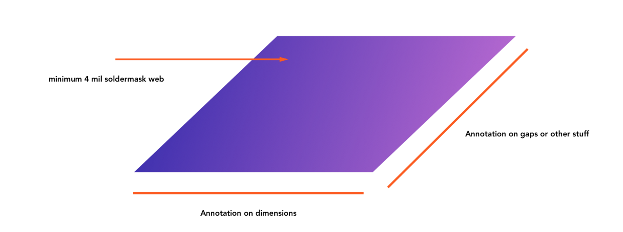
Set Solder Mask Clearance to 0.0508mm, (0.002in).
All other values can be set to 0.
Optionally, you may increase Solder Mask Min Width to 0.101mm (0.004in). A value above 0 will remove soldermask between fine pitch pins.
Design Rules Editor
Open the Design Rules Editor by going to Design Rules -> Design Rules in the top menu. The Design Rules Editor has two sections, and you’ll want to edit both.
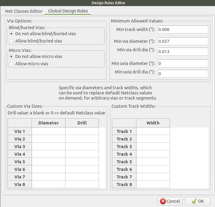
Global Design Rules tab
Since we cannot fabricate blind or buried vias, they must be disabled with the following options:
- Select
Do not allow blind/buried vias - Select
Do not allow micro vias.
The exact values Min Track Width and Via Diameter depend on the Fabrication Service.
For our 2 layer boards service with Imperial units good options are
Min track width:0.006Min via diameter:0.020(corresponding to a 5 mil annular ring)Min via drill diameter:0.010
To calculate the Min Via diameter, use the formula (minimum drill diameter) + (annular ring spec)*2
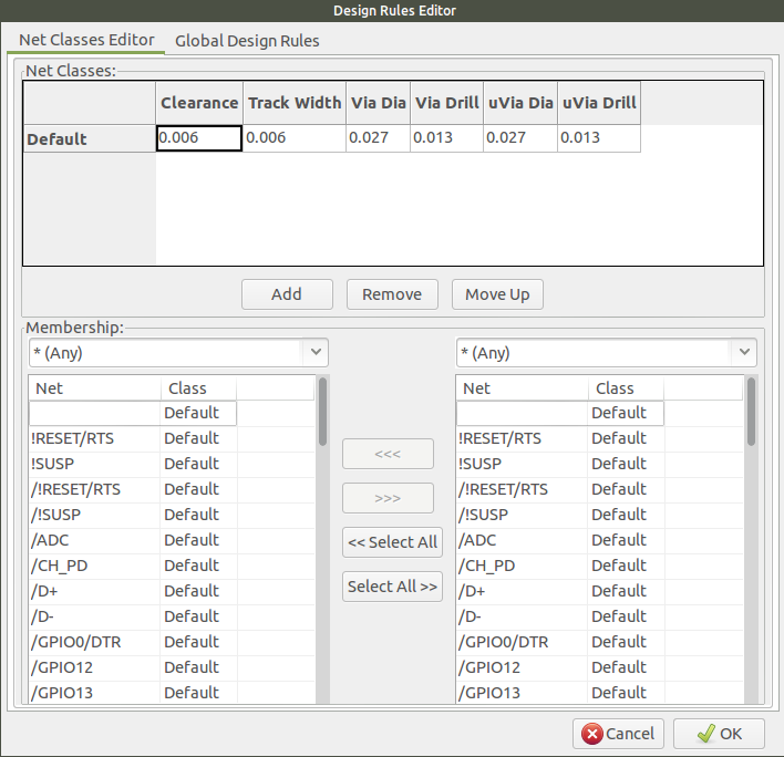
Net Classes Editor tab
You can configure the Default net class with the same settings as above.
Since Kicad requires a value for uVia Dia and uVia Drill, we suggest use the same as Via dia and Via Drill. However, these will be ignored since uVias are disabled.
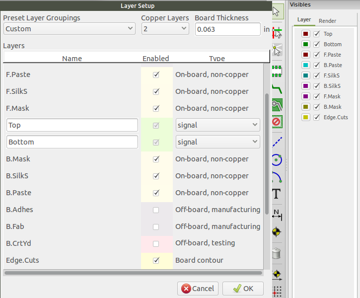
Layer Setup
Under Design Rules -> Layer Setup is a list of layers that you can Enable or Disable. The important fabrication layers to enable are as follows:
F.SilksF.MaskF.CuB.CuB.MaskB.SilksEdge.Cutswhich contains the board outline.In1.CuandIn2.Cuare also needed for 4 layer designs.
F.Paste and B.Paste are optional manufacturing layers, and are useful when ordering solder paste stencils.
Several other layers also have helpful purposes when designing a board, and you can disable or enable if you’d like:
Marginwhich shows you the edge of board clearancesF.CrtYdandB.CrtYdwhich indicates suggested clearances around individual componentsCmts.Useris for user comments which is helpful for making notes and references on a non-manufacturing layer.