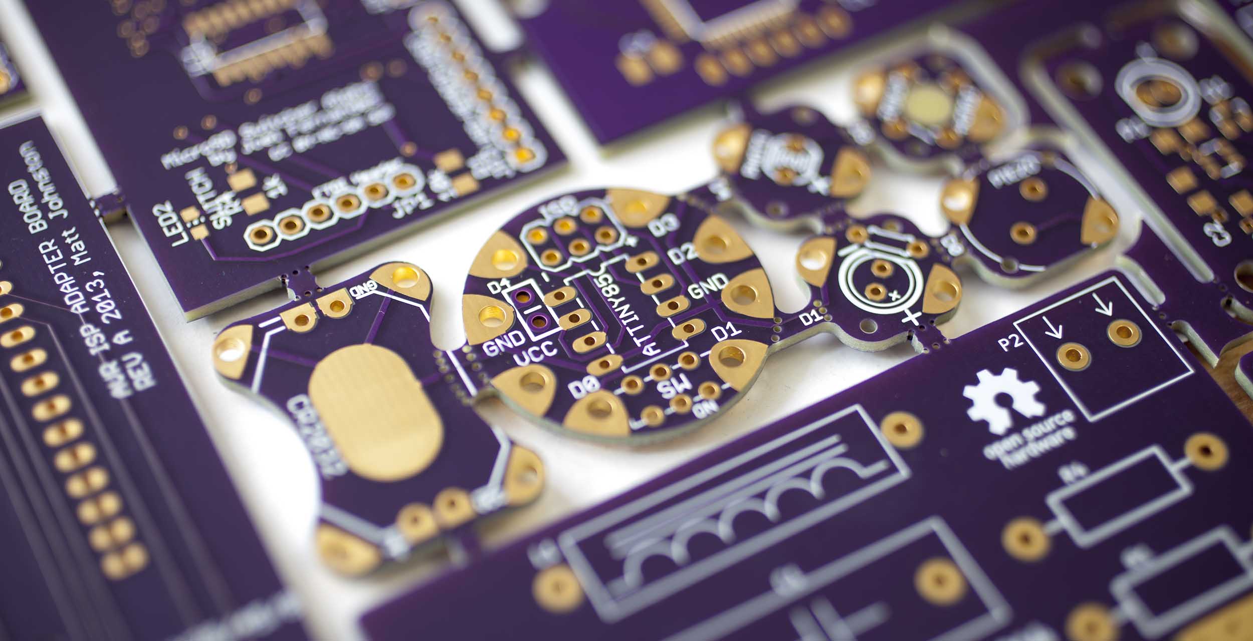
2 Layer Prototype Service
Our famous 2 layer purple prototype production.
Pricing
$5 per square inch, which includes three copies of your design. For example, a 2 square inch board would cost $10 and you’d get three copies of your board. You can order as many copies as you want, as long as they’re in multiples of three.
Turn Times
Orders are sent to fabrication daily, and will ship within 9-12 calendar days. 90% of our 2 layer orders ship in 10 calendar days.
You can get a quote, approve a design, and pay for an order at OSH Park.
For a faster turn time, you may be interested in our Super Swift Service.
For thinner, lighter, or high current boards, you may be interested in our 2oz-0.8mm Service.
Need more than 100 square inches of boards? Our 2 Layer Medium Run Service is a less expensive option for larger orders.
Common Specs
These specs apply to all our PCB services.
| Spec | Value | |
|---|---|---|
| Manufactured in the United States | Yes | |
| Lead Free compatible | Yes | |
| RoHS Compliant | Yes | |
| High Temp | Yes, 175 Tg or higher (see Material Specs) | |
| PCB Finish | ENIG (Gold), compliant with IPC-4552 | |
| Soldermask Type | SMOBC (Soldermask Over Bare Copper), both sides | |
| Silkscreen Type | High Res DLP, both sides |
Stackup
| Thickness | Layer | Tolerance |
|---|---|---|
| 0.6 mil (0.0152mm) | silkscreen | +/-0.2mil (0.00508mm) |
| 0.6 mil (0.0152mm) | solder resist | +/-0.2mil (0.00508mm) |
| 1.4 mil (0.0356mm) | 1 oz copper | |
| 60 mil (1.5240mm) | core | +/-6mil (0.1524mm) |
| 1.4 mil (0.0356mm) | 1 oz copper | |
| 0.6 mil (0.0152mm) | solder resist | +/-0.2mil (0.00508mm) |
| 0.6 mil (0.0152mm) | silkscreen | +/-0.2mil (0.00508mm) |
Material Specs
| Spec | Value | |
|---|---|---|
| Substrate | 175Tg FR4 | Kingboard KB6167F Datasheet |
| Board Thickness | 63mil (1.6mm) nominal | |
| Dielectric | 4.5 at 10Mhz | |
| Soldermask Color | Purple | Mask Datasheet |
| Minimum soldermask web | 4 mil (0.1016mm) | |
| Maximum soldermask alignment | 3mil (0.0762mm) | Covers retraction, expansion, and shift |
| Silkscreen minimum line width | 5 mil (0.127mm) (recommended minimum) 3 mil (0.0762mm) (short lines, text, graphics) |
Silkscreen Datasheet |
| Maximum board size | 16in (406.4mm) by 22in (558.8mm) | |
| Minimum board size | 0.25in (6.35mm) by 0.25in (6.35mm) |
Copper Specifications
| Spec | Value | |
|---|---|---|
| Copper Layers | 2 | |
| Copper Weight | 1oz | |
| Trace Spacing | 6mil (0.1524mm) | |
| Trace Width | 6mil (0.1524mm) | |
| Annular Ring | 5mil (0.127mm) | |
| Board Edge Keepout | 15mil (0.381) from nominal board edge | |
| Via Plating Thickness | 1mil (0.0254mm) |
Drill Specifications
| Spec | Value | |
|---|---|---|
| Minimum Annular Ring | 5mil (0.127mm) | |
| Minumum Drill Size | 10mil (0.254mm) | |
| Minimum Slot Size | 20mil (0.508mm) (drill slot only) | Additional information on slots |
| Milling tool diameter | Outline/profile milling: 0.068” (1.72mm) Interior/cutout milling: 0.040” (1.01mm) |
Additional outline/profile detail |
| Drill Size tolerance | Max: +/- 2.5mil (0.0635mm) Typical: +/- 1.0mil (0.0254) |
|
| Drill Positional Tolerance | Max: 2mil (0.0508mm) Typical: <1mil (0.0254mm) |
|
| Via Tenting | Yes (filled hole and flat surface not guaranteed) | |
| Buried Via | No | |
| Blind Via | No | |
| Filled+Plated Vias (via-in-pad) | No | |
| Overlapping drills | Allowed, but not guaranteed. May result in missing or slotted holes. 5 mil (0.127mm) clearance is recommended between holes. |
|
| Castellations | Allowed, but not guaranteed | Details and recommendations |
| Maximum Drill Size | None | Drill sizes above 250mil (6.35mm) will be fabbed, but with larger milling tolerances. |
