2 Layer Medium Run Service
Moving to a small production run? Our medium run service will help bridge the gap between prototypes and a full panel.
Pricing
$1 per square inch, 100 square inch minimum. You can have as many different designs as you want, as long as each design is ordered in a multiple of 10 boards.
For example, if you had two different 5 square inch designs, you could order 10 of each for a total cost of $100.
100 inches is just the minimum order. You can order as much as you’d like beyond that.
Turn Times
Orders will be shipped within 12-21 calendar days of ordering.
Medium Run orders cannot be expedited. For faster fabrications options, you may be interested in our 2 Layer Service or even faster 2 Layer Super Swift Service.
You can get a quote, approve a design, and pay for an order at OSH Park.
Common Specs
These specs apply to all our PCB services.
| Spec | Value | |
|---|---|---|
| Manufactured in the United States | Yes | |
| Lead Free compatible | Yes | |
| RoHS Compliant | Yes | |
| REACH Compliant | Yes | |
| High Temp | Yes, 175 Tg or higher (see Material Specs) | |
| PCB Finish | ENIG (Gold), compliant with IPC-4552 | |
| Soldermask Type | SMOBC (Soldermask Over Bare Copper), both sides | |
| Silkscreen Type | High Res DLP, both sides | |
| Flammability Rating | UL 94 V-0 |
Stackup
| Thickness | Layer | Tolerance |
|---|---|---|
| 0.6 mil (0.0152mm) | silkscreen | +/-0.2mil (0.00508mm) |
| 0.6 mil (0.0152mm) | solder resist | +/-0.2mil (0.00508mm) |
| 1.4 mil (0.0356mm) | 1 oz copper | |
| 60 mil (1.5240mm) | core | +/-6mil (0.1524mm) |
| 1.4 mil (0.0356mm) | 1 oz copper | |
| 0.6 mil (0.0152mm) | solder resist | +/-0.2mil (0.00508mm) |
| 0.6 mil (0.0152mm) | silkscreen | +/-0.2mil (0.00508mm) |
Material Specs
| Spec | Value | |
|---|---|---|
| Substrate | 175Tg FR4 | Kingboard KB6167F Datasheet |
| Board Thickness | 63mil (1.6mm) nominal | |
| Dielectric | 4.5 at 10Mhz | |
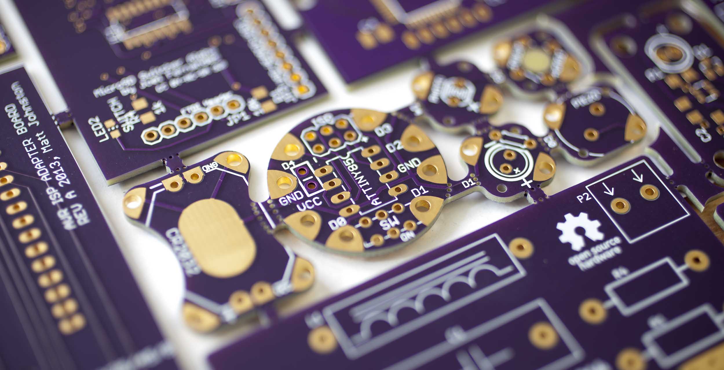
| Soldermask Color | Purple | Mask Datasheet |
| Minimum soldermask web | 4 mil (0.1016mm) | |
| Maximum soldermask alignment | 3mil (0.0762mm) | Covers retraction, expansion, and shift |
| Silkscreen minimum line width | 5 mil (0.127mm) (recommended minimum) 3 mil (0.0762mm) (short lines, text, graphics) |
Silkscreen Datasheet |
| Maximum board size | 16in (406.4mm) by 22in (558.8mm) | |
| Minimum board size | 0.25in (6.35mm) by 0.25in (6.35mm) |
Copper Specifications
| Spec | Value | |
|---|---|---|
| Copper Layers | 2 | |
| Copper Weight | 1oz | |
| Trace Spacing | 6mil (0.1524mm) | |
| Trace Width | 6mil (0.1524mm) | |
| Annular Ring | 5mil (0.127mm) | |
| Board Edge Keepout | 15mil (0.381) from nominal board edge | |
| Via Plating Thickness | 1mil (0.0254mm) |
Drill Specifications
| Spec | Value | |
|---|---|---|
| Minimum Annular Ring | 5mil (0.127mm) | |
| Minimum Drill Size | 10mil (0.254mm) | |
| Minimum Slot Size | 20mil (0.508mm) (drill slot only) | Additional information on slots |
| Milling tool diameter | Outline/profile milling: 0.068” (1.72mm) Interior/cutout milling: 0.040” (1.01mm) |
Additional outline/profile detail |
| Drill Size tolerance | Max: +/- 2.5mil (0.0635mm) Typical: +/- 1.0mil (0.0254) |
|
| Drill Positional Tolerance | Max: 2mil (0.0508mm) Typical: <1mil (0.0254mm) |
|
| Via Tenting | Yes (filled hole and flat surface not guaranteed) | |
| Buried Via | No | |
| Blind Via | No | |
| Filled+Plated Vias (via-in-pad) | No | |
| Overlapping drills | Allowed, but not guaranteed. May result in missing or slotted holes. 5 mil (0.127mm) clearance is recommended between holes. |
|
| Castellations | Allowed, but not guaranteed | Details and recommendations |
| Maximum Drill Size | None | Drill sizes above 250mil (6.35mm) will be fabbed, but with larger milling tolerances. |
