DesignSpark
DesignSpark is a free downloadable PCB design tool.
Design Rules
DesignSpark collects design rules in a Technology file for both the Schematic Design and the PCB Design. We’ve created 2 layer and 4 layer PCB Technology files that match our design specs. You can download them with instructions here.
Generating Gerbers and Drill Files
We have a full walkthrough showing how to generate Manufacturing Plots. Our system will pick up the default filenames, so if you’ve already generated them you won’t need to rename anything.
We need the drills exported in the 2:4 inches format or a 3:3 metric format, but there are a couple of other related settings to check. When you upload the zip file, you’ll have a chance to inspect and approve preview images of each layer. If something looks strange with your drill file layer, take a look at our DesignSpark Drill File CAM configuration page.
DesignSpark also incorrectly adds Outline data to the Drill files by default. While uncommon, it’s possible for this data to result in board errors in some designs, and it is recommended to check our CAM Configuration page for how to avoid this.
Board Outline
We need a watertight board outline on its own layer with no other text, measurements, or symbols. If this layer is not present, our Gerber Walkthrough will help you generate this file.
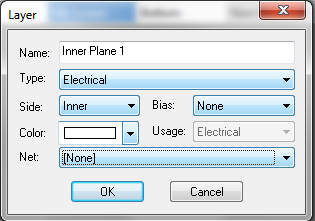
Inverted Inner Planes for 4 Layer Boards
We expect all copper layers to be submitted with positive polarity, but DesignSpark will create negative layers if your internal layers are generated as powerplanes. Unfortunately, this means we’ll place the copper in the opposite way from how you intended. See here for a better explanation.
It’s best when creating your Technology File for a new PCB Design to set the inner planes to be Electrical with a Bias: None so the inner planes are created and plotted like any other regular signal layer. If you use our Technology Files, we’ll set this up automatically for four layer designs.