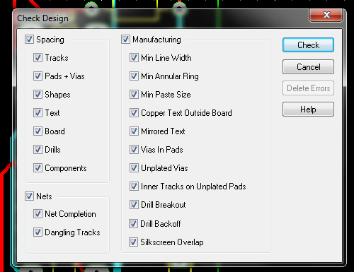
Design Rule Check
Save the Technology Files
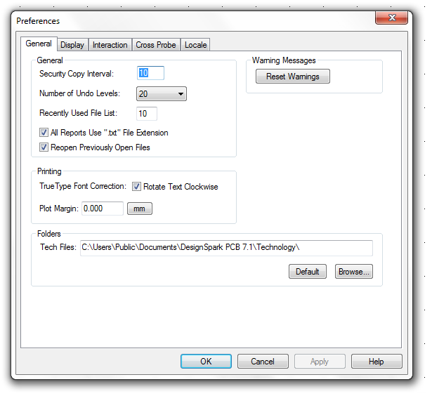
Before you save our Technology files, you need to find the folder where DesignSpark will look for them by checking the Preferences tab under Settings.
In this case, it’s C:\Users\Public\Documents\DesignSpark PCB 7.1\Technology\, so save both of these design rules files to that folder:
Load the Technology File for your PCB Design
When you’ve created and filled out your schematic, the next step is to
create the PCB Design. File > New brings up the New Design dialog.

Select PCB Design and Add to Open Project.
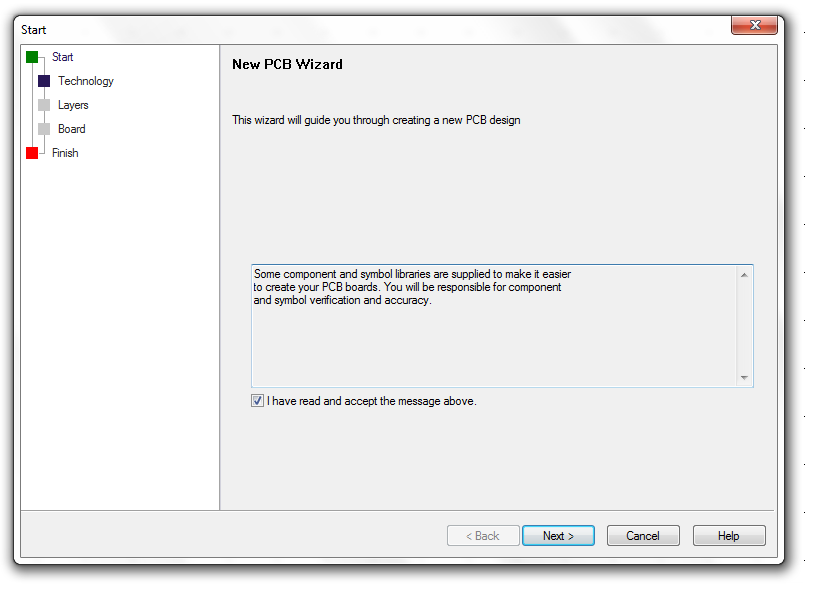
Follow the dialogs and select the OSH Park 2 or 4 layer Technology file.
Select Use the Layers from Chosen Technology File
Run the Design Rules Check
After you’ve created your PCB layout, you’ll want to run the actual check.