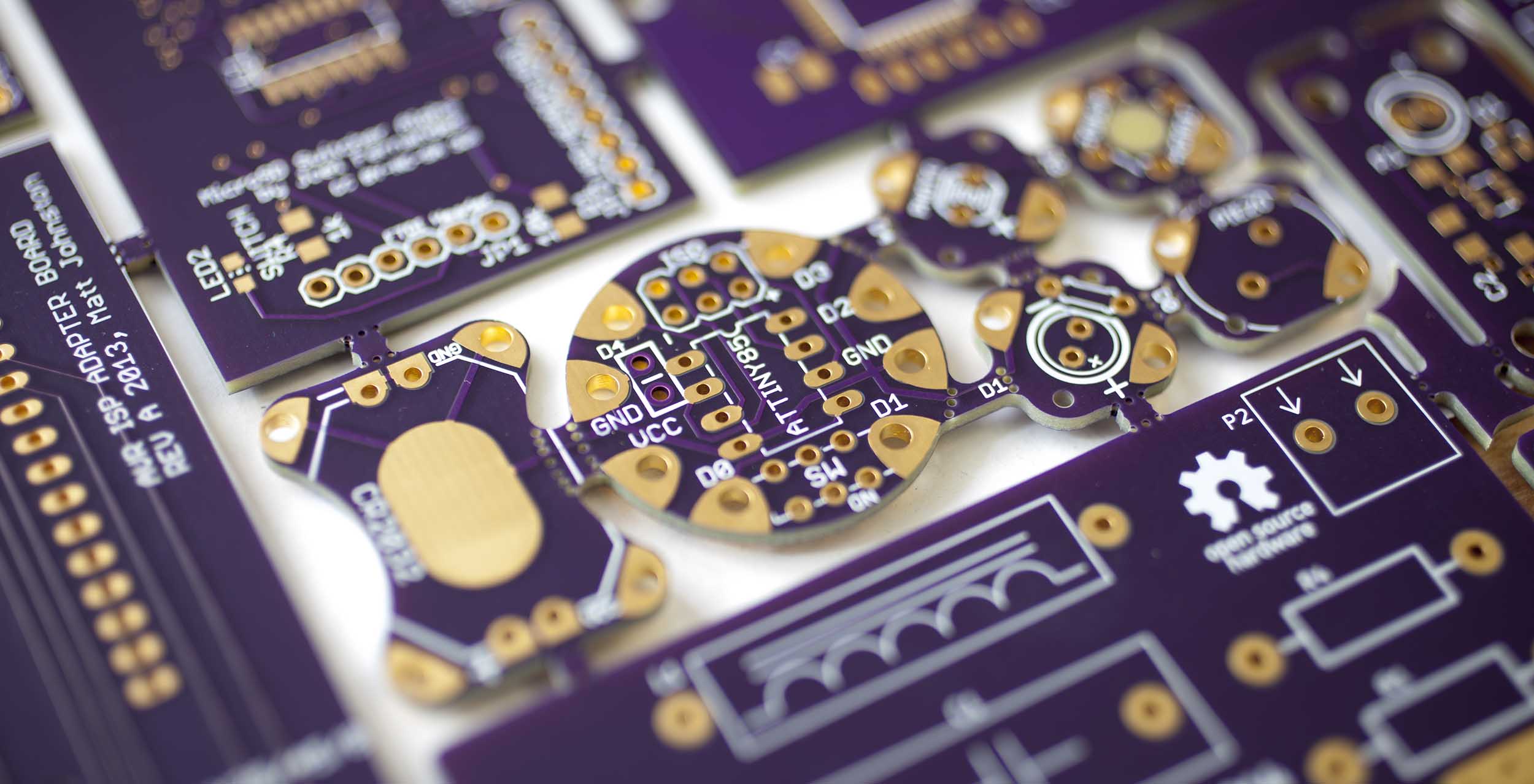
4 Layer Prototype Service
Pricing
$10 per square inch, which includes three copies of your design.
For example, a 2 square inch board would cost $20 and you’d get three copies of your board. You can order as many copies as you want, as long as they’re in multiples of three.
Turn Times
Orders will ship within 9-14 calendar days of ordering.
You can get a quote, approve a design, and pay for an order at OSH Park.
For a faster turn time, you may be interested in our 4 Layer Super Swift Service.
Need more than 100 square inches of boards? Our 4 Layer Medium Run Service is a less expensive option for larger orders.
Common Specs
These specs apply to all our PCB services.
| Spec | Value | |
|---|---|---|
| Manufactured in the United States | Yes | |
| Lead Free compatible | Yes | |
| RoHS Compliant | Yes | |
| REACH Compliant | Yes | |
| High Temp | Yes, 175 Tg or higher (see Material Specs) | |
| PCB Finish | ENIG (Gold), compliant with IPC-4552 | |
| Soldermask Type | SMOBC (Soldermask Over Bare Copper), both sides | |
| Silkscreen Type | High Res DLP, both sides | |
| Flammability Rating | UL 94 V-0 |
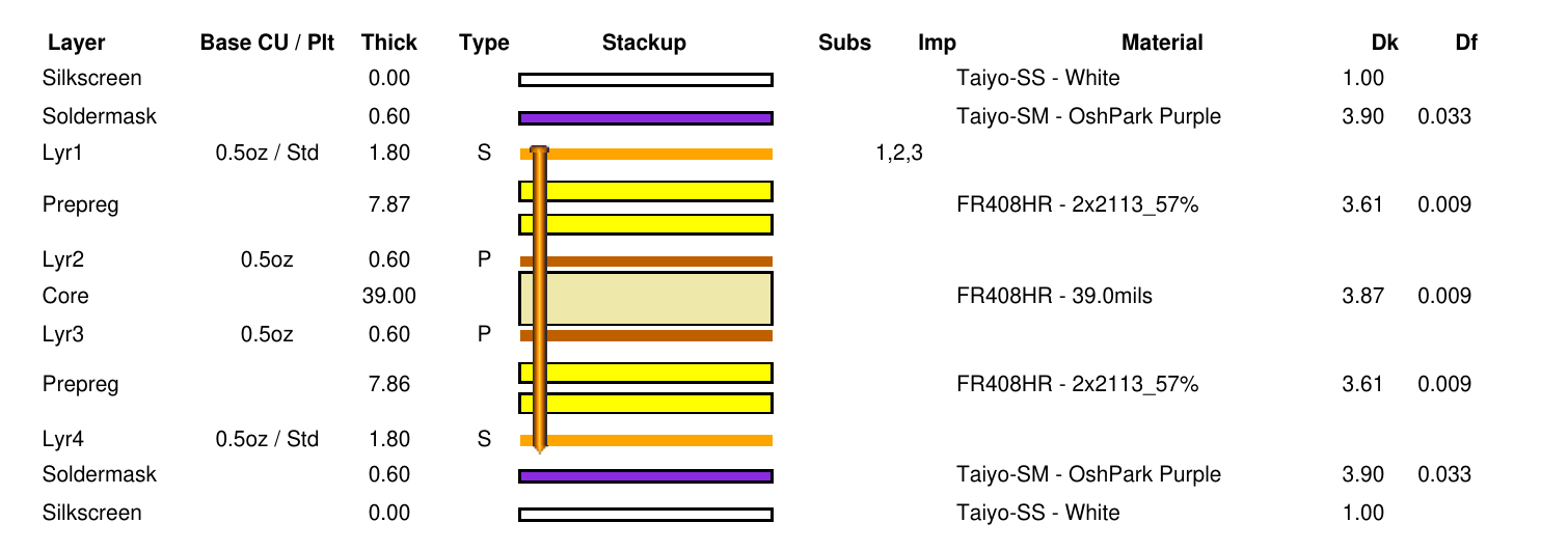
Stackup
| Thickness | Layer | Tolerance | dk |
|---|---|---|---|
| 0.6 mil (0.0152mm) | silkscreen | +/-0.2mil (0.00508mm) | |
| 0.6 mil (0.0152mm) | solder resist | +/-0.2mil (0.0051mm) | |
| 1.7 mil (0.0432mm) | 1 oz copper clad+plated | ||
| 7.87 mil (0.1999mm) | FR408HR 2113 prepreg | +/-.797mil (0.0202mm) | 3.61 at 1GHz |
| 0.68 mil (0.0175mm) | 0.5 oz copper clad | ||
| 39 mil (0.9906mm) | FR408HR core |
+/-3.9mil (0.0991mm) | |
| 0.68 mil (0.0175mm) | 0.5 oz copper clad | ||
| 7.87 mil (0.1999mm) | FR408HR 2113 prepreg | +/-.797mil (0.0202mm) | 3.61 at 1GHz |
| 1.7 mil (0.0432mm) | 1 oz copper clad+plated | ||
| 0.6 mil (0.0152mm) | solder resist | +/-0.2mil (0.0051mm) | |
| 0.6 mil (0.0152mm) | silkscreen | +/-0.2mil (0.00508mm) |
For orders fabricated on the alternate stackup between 2025-Dec-20 and 2026-Jan-28, you can find additional information here: EM528 Alternate Stackup. These boards will have a red core, instead of the white core we generally use.
Material Specs
| Spec | Value | |
|---|---|---|
| Substrate | 190Tg FR408-HR | ISOLA FR408-HR Datasheet PDF |
| Board Thickness | 63mil (1.6mm) nominal | |
| Dielectric | 3.61 at 1GHz | |
| Soldermask Color | Purple | Mask Datasheet |
| Minimum soldermask web | 4 mil (0.1016mm) | |
| Maximum soldermask alignment | 3mil (0.0762mm) | Covers retraction, expansion, and shift |
| Silkscreen minimum line width | 5 mil (0.127mm) (recommended minimum) 3 mil (0.0762mm) (short lines, text, graphics) |
Silkscreen Datasheet |
| Maximum board size | 16in (406.4mm) by 22in (558.8mm) | |
| Minimum board size | 0.25in (6.35mm) by 0.25in (6.35mm) |
Copper Specifications
| Spec | Value | |
|---|---|---|
| Copper Layers | 4 | |
| Copper Weight | 1oz outer 1/2oz inner |
|
| Trace Spacing | 5mil (0.127mm) | |
| Trace Width | 5mil (0.127mm) | |
| Annular Ring | 4mil (0.1016mm) | |
| Board Edge Keepout | 15mil (0.381) from nominal board edge | |
| Via Plating Thickness | 1mil (0.0254mm) | |
| Plated Drill to Internal Layer Copper Clearance | 10mil (0.254mm) |
Drill Specifications
| Spec | Value | |
|---|---|---|
| Minimum Annular Ring | 4mil (0.1016mm) | |
| Minimum Drill Size | 10mil (0.254mm) | |
| Minimum Slot Size | 20mil (0.508mm) (drill slot only) | Additional information on slots |
| Milling tool diameter | Outline/profile milling: 0.068” (1.72mm) Interior/cutout milling: 0.040” (1.01mm) |
Additional outline/profile detail |
| Drill Size tolerance | Max: +/- 2.5mil (0.0635mm) Typical: +/- 1.0mil (0.0254) |
|
| Drill Positional Tolerance | Max: 2mil (0.0508mm) Typical: <1mil (0.0254mm) |
|
| Via Tenting | Yes (filled hole and flat surface not guaranteed) | |
| Buried Via | No | |
| Blind Via | No | |
| Filled+Plated Vias (via-in-pad) | No | |
| Overlapping drills | Allowed, but not guaranteed. May result in missing or slotted holes. 5 mil (0.127mm) clearance is recommended between holes. |
|
| Castellations | Allowed, but not guaranteed | Details and recommendations |
| Maximum Drill Size | None | Drill sizes above 250mil (6.35mm) will be fabbed, but with larger milling tolerances. |
| Plated Drill to Internal Layer Copper Clearance | 10mil (0.254mm) |
Outgassing
| Material | TML % | CVCM % | WVR % |
|---|---|---|---|
| FR408HR | 0.11% | 0.01% | 0.10% |
Isola Outgassing documentation
Layer Naming
We automatically detect intended layer order from many tools, using common naming conventions and meta-data formats like Gerber X2. In most cases, renaming files should not be needed, and you can use your default export settings.
If your tool or files requires configuration or manual renaming of layers, we suggest this pattern to ensure your layer order is interpreted correctly.
| Layer | Suggested File Extension | |
|---|---|---|
| Layer 1 | .GTL | Top or Front layer |
| Layer 2 | .G2L | Internal layer (adjacent to Top) |
| Layer 3 | .G3L | Internal layer (adjacent to Bottom) |
| Layer 4 | .GBL | Bottom or Back layer |
For additional info or other layers, see our Suggested Naming Pattern
Internal Plane Polarity
When submitting gerbers, we need the “positive” internal planes, meaning that lines represent copper, not the absence of copper.
Some CAD tools will generate the internal planes as power planes with “negative” polarity so the lines indicate where copper should be removed. To work around this, declare the internal planes as signal layers and use a copper pour to define the power plane.
In most cases, our software will detect and resolve this automatically during our pre-production steps.
Take a look at our Positive and Negative Gerbers page for more information.
Drill Internal Layer Clearance
Some tools will often suppress annular rings on vias that do not connect to internal layers. However, this may not accurately capture required production specs, leading to inadvertent spec violations. While these violations do not always result in issues, they can lead to surprising defects and yield issues.
This DRC requirement is not always obvious inside design tools, with some tools defaulting to a violation, and not providing clear warnings. Care should be taken to ensure compliance. Tools handle this differently, but one of the following methods should help:
- Configuring the tool to always include annular rings, regardless of net connections
- Increasing ground plane clearance on internal layer copper pours
- Configuring custom net rules to increase isolation on internal layer copper pours.
Your design tool’s documentation will assist with these steps.


Changelog
28-JAN-2026 Added notes regarding the temporary alternate stackup used for some 4 layer orders.
9-SEP-2025 Removed notice for stackup change, as no stackup change will be occouring.
27-AUG-2025 Added notice for potential future stackup change due to concern regarding material availabillity
25-JUL-2024 Corrected prepreg thickness from 7.96mil to 7.87mil to better match the boards as fabricated. This is a documentation correction, and does not reflect a production change.
17-JUN-2024 Added DRC item for vias passing through internal layers without generating annular rings.
